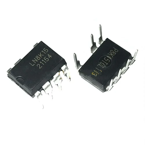
SOP8Новий


Ірпінська, 74
093 150 30 72
096 550 30 37
ПН - ПТ з 12.00 до 17.00
50,00 грн
34 в наявності
34 в наявності
Мікросхема STC8G1K08 SOP8
STC8G-EN – даташит у нас на сайті
Microcontroller MCU
Ultra-high speed 8051 Core with single clock per machine cycle, which is called 1T and the speed is about 12 times faster than traditional 8051
Fully compatible instruction set with traditional 8051
13 interrupt sources and 4 interrupt priority levels
Online debugging is supported
1.9V~5.5V
Built-in LDO
-40℃~85℃
Up to 17K bytes of Flash memory to be used to store user code STC8G Series Manual
Configurable size EEPROM, 512bytes single page erased, can be repeatedly erased more than 100 thousand times.
In-System-Programming, ISP in short, can be used to update the application code, no need for special programmer.
Online debugging with single chip is supported, and no special emulator is needed. The number of breakpoints is unlimited theoratically.
128 bytes internal direct access RAM (DATA)
128 bytes internal indirect access RAM (IDATA)
1024 bytes internal extended RAM (internal XDATA)
Internal high precise R/C clock (IRC, range from 4MHz to 36MHz), adjustable while ISP and can be divided to lower frequency by user software, 100KHz for instance.
Error:±0.3% (at the temperature 25℃)
-1.38% – +1.42% temperature drift (at the temperature range of -40°C to +85°C)
-0.88% – +1.05% temperature drift (at the temperature range of -20℃ to 65℃)
Internal 32KHz low speed IRC with large error
Hardware reset
Power-on reset. Measured voltage value is 1.69V~1.82V. (Effective when the chip does not enable the low voltage reset function) The power-on reset voltage is a voltage range consisting of an upper limit voltage and a lower limit voltage. When the operating voltage drops from 5V / 3.3V to the lower limit threshold voltage of the power-on reset, the chip is in a reset state; when the voltage rises from 0V to the upper threshold voltage of power-on reset, the chip is released from the reset state.
Reset by reset pin. The default function of P5.4 is I/O port. The P5.4 pin can be set as the reset pin while ISP download. (Note: When the P5.4 pin is set as the reset pin, the reset level is low.)
Watch dog timer reset
Low voltage detection reset. 4 low voltage detection levels are provided, 2.2V (Measured as 1.90V~2.04V), 2.4V (Measured as 2.30V~2.50V), V2.7 (Measured as 2.61V~2.82V), V3.0 (Measured as 2.90V~3.13V). Each level of low-voltage detection voltage is a voltage range consisting of an upper limit voltage and a lower limit voltage. When the operating voltage drops from 5V / 3.3V to the lower limit threshold voltage of low-voltage detection, the low-voltage detection takes effect. When the voltage rises from 0V to the upper threshold voltage, the low voltage detection becomes effective.
Software reset
Writing the reset trigger register using software
13 interrupt sources: INT0(Supports rising edge and falling edge interrupt), INT1(Supports rising edge and falling edge interrupt), INT2(Supports falling edge interrupt only), INT3(Supports falling edge interrupt only), INT4(Supports falling edge interrupt only), timer0, timer1, UART1, ADC, LVD, SPI, I 2C, PCA/CCP/PWM
4 interrupt priority levels
Interrupts that can awaken the CPU in clock stop mode: INT0 (P3.2), INT1 (P3.3), INT2 (P3.6), INT3 (P3.7), INT4 (P3.0), T0 (P3.4), T1(P3.5), RXD(P3.0/P3.2/P1.6/P5.4), CCP0(P3.2/P3.1), CCP1 (P3.3), CCP2 (P5.4/P5.5), I2C_SDA (P3.3/P5.5) and low-voltage detection interrupt, power-down wake-up timer.
2 16-bit timers: timer0, timer1, where the mode 3 of timer0 has the Non Maskable Interrupt (NMI in short) function. Mode 0 of timer0 and timer1 is 16-bit Auto-reload mode.
1 high speed UART: UART1, whose baudrate clock may be fast as FOSC/4
3 groups of PCAs: CCP0, CCP1, CCP2, which can be used as capture, high speed output and 6-bits, 7-bits, 8-bits or 10-bits PWM.
SPI: Master mode, slave mode or master/slave automatic switch mode are supported.
I 2C: Master mode or slave mode are supported.
MDU16: Hardware 16-bit Multiplier and Divider which supports 32-bit divided by 16-bit, 16-bit divided by 16-bit, 16-bit by 16-bit, data shift, and data normalization operations.
6 channels (channel 0 to channel 5) ultra-high speed ADC which supports 10-bit precision analog-to-digital conversion, the speed can be as fast as 500K(500,000 conversions per second).
ADC channel 15 is used to test the internal reference voltage. (The default internal reference voltage is 1.19V when the chip is shipped)
DAC. 3 groups of PCAs can be used as DAC.
Up to 6 GPIOs: P3.0~P3.3, P5.4~P5.5
4 modes for all GPIOs: quasi_bidirectional mode, push-pull outputmode, open drain mode, high-impedance input mode
Except for P3.0 and P3.1, all other I/O ports are in a high-impedance state after power-on. User must set the I/O ports mode before using them. In addition, each I/O can independently enable the internal 4K pullup resistor.
SOP8, DFN8 (3mm*3mm), DIP8